RAM
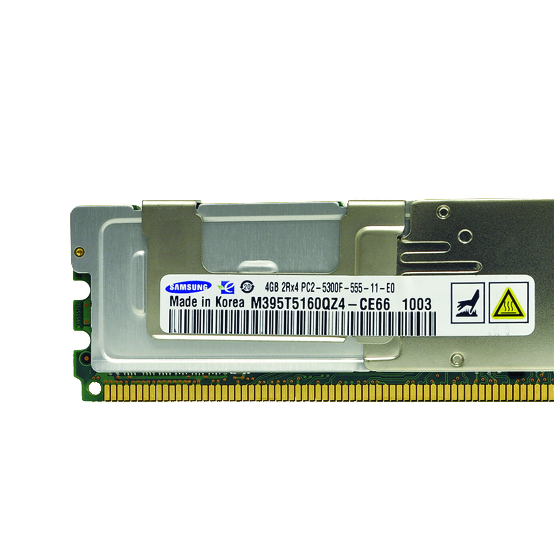
The MasterServer features 24 GB of Samsung FDB-533/PC25300F FB-DDR2 ECC RAM.
Features
| Feature | Value |
|---|---|
| Size | 4 GB |
| Frequency | 333 MHz * |
| Voltage | 1,8V |
| JEDEC Timings (CL-tRCD-tRP-tRAS-tRC) | 5-5-5-15-20 |
| Release | 2008 |
Note
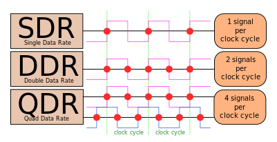
Due to DDR, the effective RAM frequency is 667 MHz
DIMMs
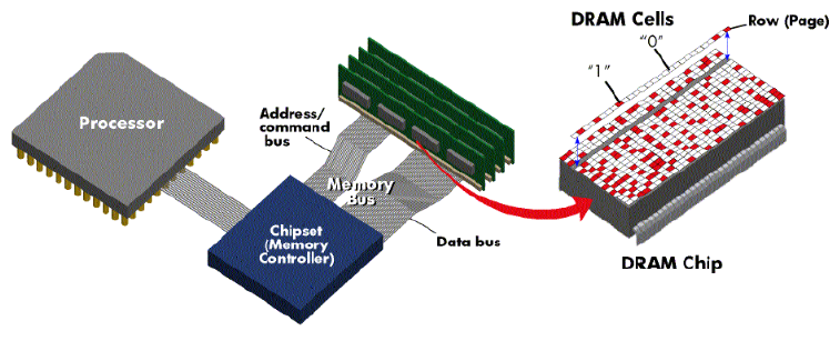
A DIMM is a Dual In-Line Memory Module.
Compared to its older version, SIMM, they have pins on both of their sides, pair by pair. Anyway, the DRAM chips technology is the same.
Traditional DIMMs
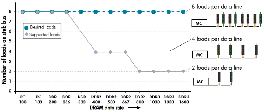
Traditional DIMM architectures use the stub-bus topology.
Each DIMM connects with the shared memory bus via parallel branches (stubs). The traces must be the same length (Traces between the MCH and the memory slots are usually circuitous) so electrical signals from the Memory Controller are able to reach the DIMMs at the same time.
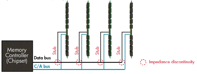
Each stub-bus connection creates resistance that degrades signal integrity and creates an electrical load on the bus.
Adding more DIMMs result in an increase on the load, and higher data rates [1] support less loads per channel.
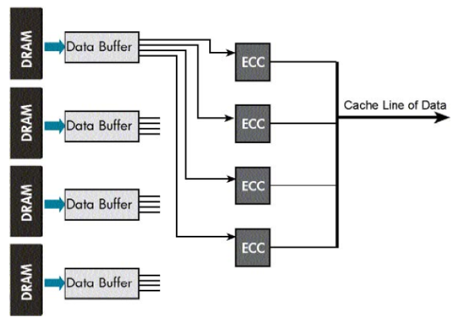
Fully Buffered DIMMs
FB-DIMMs are Fully Buffered DIMMs, which means each DIMM has its own buffer.
They work in a different way compared to regular DIMMs and its specification was developed by the JEDEC [2].
A serial interface connected to the Memory Controller in a daisy chain [3] configuration that eliminates the parallel stub-bus topology and allows higher memory bandwidth and capacity.
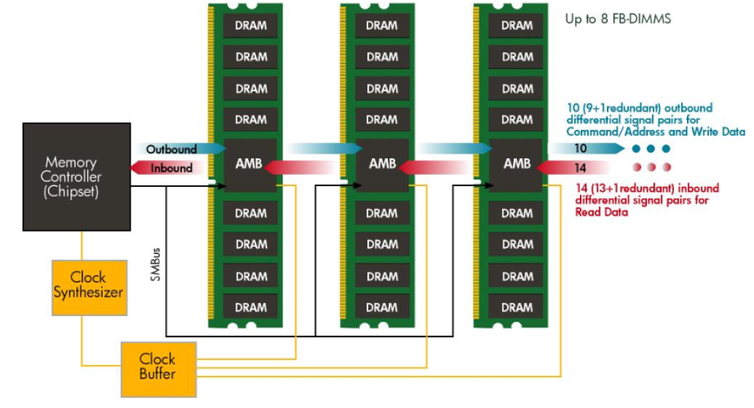
The serial links connect the MCH to the Advanced Memory Buffer or AMB, located in each memory stick creating a point-to-point architecture.
Outbound links trasmit commands and write data to the FB-DIMMs while inbound links transmit read data back to the MCH.
Note
Due to production costs, power requirements and latency, FB-DIMMs have been replaced by the NUMA architecture
ECC
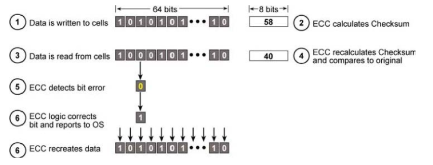
Error Correction Code is a technology used in RAM or any kind of communications to detect an error and correct it. Other technologies like EDC [4] only detect when there’s an error but don’t fix it.
Basic ECC
Its parity checking detects only single-bit errors and does not correct multi-bit or memory errors. It was introduced circa 1993.
Advanced ECC
It’s an improvement beyond the standard ECC introduced in 1996. It can correct multi-bits errors and avoid complete DRAM failures.
A comparison of both technologies is shown below.
| Error Condition | ECC Outcome | Advanced ECC Outcome |
|---|---|---|
| Single-bit | Correct | Correct |
| Double-bit | Detect | Correct Or Detect |
| DRAM Failure | Detect | Correct |
UMA & NUMA
In computing there are 2 major parallel architectures; Shared Memory Architecture and Distributed Memory Architecture
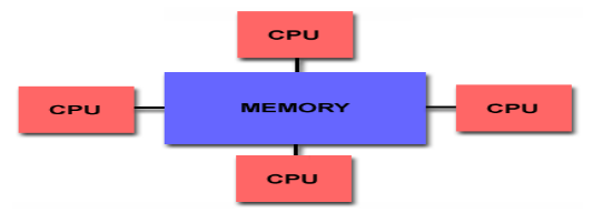
- Shared Memory Architecture; All processors share the same memory and treat it as a global address space, dealing with cache coherency and global memory address space . Its used on single PCs
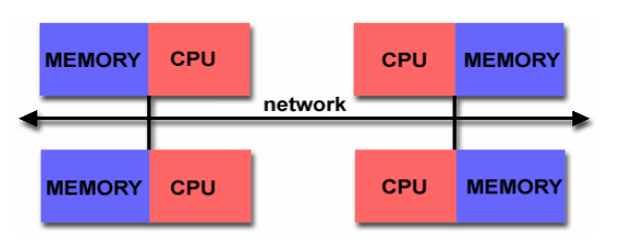
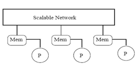
- Distributed Memory Architecture; All processors have their own local memory without memory addresses mapping across processors. Its used with clusters
There are 2 types of Shared Memory Architecture;
- UMA (Uniform Memory Access); Memory design used for SMP [5] systems where the memory access time depends on the bus or MCH
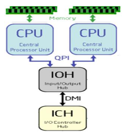
- NUMA (Non-Uniform Memory Access); Memory design used for multiCPU or SMP systems where the memory access time depends on the distance between the RAM and CPU
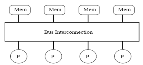
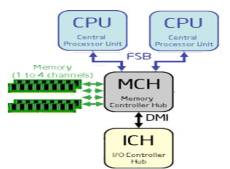
UMA is used by SMP computers that have an MCH. The MCH manages the memory access and interconnects the RAM and CPU through a bus. That means the memory access time is determined by the FSB frequency and bandwidth and the MCH.
Meanwhile, NUMA is used by SMP computers that have the MCH in the CPU dye. The memory access time is determined by the distance between the CPU and the RAM and the interconnect network between each CPU.
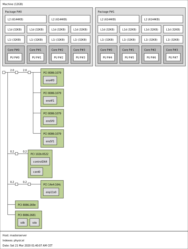
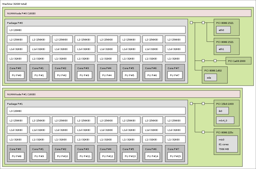
I obtained the MasterServer architecture using the program hwloc.
With the command
lstopo topology.png I generated the output in an image.Here there is a comparison between the MasterServer UMA architecture and a newer Xeon from the X5500 series NUMA architecture featuring QPI.
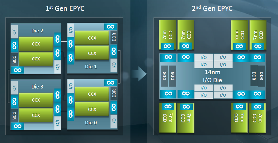
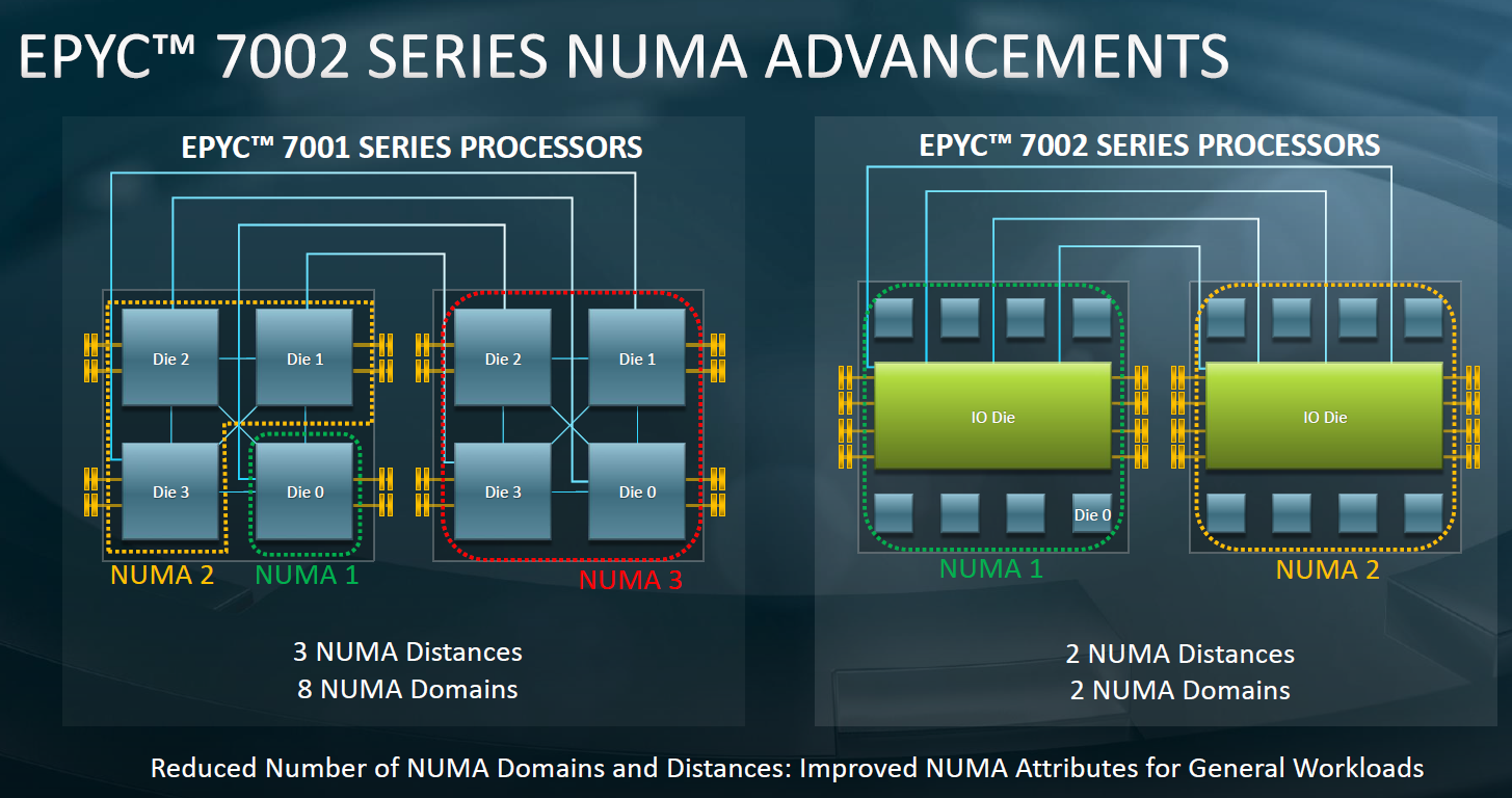
And not only that, but also the new Ryzen Threadripper took NUMA a step further; Inside the CPU dye with the chiplets architecture.
I see a huge potential implementing multiple CPUs under the same IHS [8] as the trend is to increase the number of cores.
Footnotes
| [1] | Usually measured as MHz |
| [2] | Joint Electron Device Engineering Council, standard that ensures RAM compatibility within motherboards |
| [3] | Wiring scheme in which multiple devices are wired togheter in a sequence or ring |
| [4] | Error Detection Code |
| [5] | Symmetric Multiprocessor |
| [6] | QuickPath Interconnect |
| [7] | UltraPath Inteconnect |
| [8] | Integrated Heat Spreeder |